Research
New Study Showcases 3D Photonics with Record Performance for AI
A Columbia Engineering team addresses critical challenges in data communications that persistently block how well AI hardware systems perform.
Artificial intelligence (AI) systems promise transformative advancements, yet their growth has been limited by energy inefficiencies and bottlenecks in data transfer. Researchers at Columbia Engineering have unveiled a groundbreaking solution: a 3D photonic-electronic platform that achieves unprecedented energy efficiency and bandwidth density, paving the way for next-generation AI hardware.
The study, “3D Photonics for Ultra-Low Energy, High Bandwidth-Density Chip Data Links,” led by Keren Bergman, Charles Batchelor Professor of Electrical Engineering, is published today in Nature Photonics. The research details a pioneering method that integrates photonics with advanced complementary-metal- oxide-semiconductor (CMOS) electronics to redefine energy-efficient, high-bandwidth data communication. This innovation addresses critical challenges in data movement, a persistent obstacle to realizing faster and more efficient AI technologies.
“In this work, we present a technology capable of transferring vast volumes of data with unprecedentedly low energy consumption,” said Bergman. “This innovation breaks through the long-standing energy barrier that has limited data movement in traditional computer and AI systems.”
Breakthrough in data communication
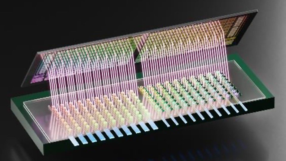
The Columbia Engineering team collaborated with Alyosha Christopher Molnar, Ilda and Charles Lee Professor of Engineering at Cornell University, to develop a 3D-integrated photonic-electronic chip that boasts a high density of 80 photonic transmitters and receivers within a compact chip footprint. This platform delivers high bandwidth (800 Gb/s) with exceptional energy efficiency, consuming just 120 femtojoules per bit. With a bandwidth density of 5.3 Tb/s/mm², this innovation far exceeds existing benchmarks.
Designed for low cost, the chip integrates photonic devices with CMOS electronic circuits and leverages components manufactured in commercial foundries, setting the stage for widespread industry adoption.
Revolutionizing AI hardware
The team’s research redefines how data is transmitted between compute nodes, addressing the long-standing bottlenecks in energy efficiency and scalability. By 3D integrating photonic and electronic chips, this technology achieves unmatched energy savings and high bandwidth density, breaking free from traditional data locality constraints. This innovative platform enables AI systems to efficiently transfer vast volumes of data, supporting distributed architectures that were previously impractical due to energy and latency limitations.
The resulting advancements are poised to unlock unprecedented levels of performance, making this technology a cornerstone of future computing systems across applications, from large-scale AI models to real-time data processing in autonomous systems. Beyond AI, this approach holds transformative potential for high-performance computing, telecommunications, and disaggregated memory systems, signaling a new era of energy-efficient, high-speed computing infrastructure.
Collaborators
The collaborative research included contributions from Cornell University’s Molnar lab, the Air Force Research Laboratory, and Dartmouth College. The project received funding from the Defense Advanced Research Projects Agency (DARPA) and the Advanced Research Projects Agency-Energy (ARPA-E), underscoring its critical role in advancing national technological capabilities.
Lead Photo Caption: 3D photonic chip module
Lead Photo Credit: Keren Bergman
About the Study
Journal: Nature Photonics
Title: 3D Photonics for Ultra-Low Energy, High Bandwidth-Density Chip Data Links
Authors: Stuart Daudlin, Anthony Rizzo, Sunwoo Lee, Devesh Khilwani, Christine Ou, Songli Wang, Asher Novick, Vignesh Gopal, Michael Cullen, Robert Parsons, Kaylx Jang, Alyosha Molnar, and Keren Bergman
Affiliations:
Department of Electrical Engineering, Columbia University
- Asher Novick
- Stuart Daudlin
- Songli Wang
- Vignesh Gopal
- Michael Cullen
- Robert Parsons
- Kaylx Jang
- Keren Bergman
Department of Electrical and Computer Engineering, Cornell University
- Sunwoo Lee
- Devesh Khilwani
- Christine Ou
- Alyosha Molnar
Air Force Research Laboratory Information Directorate
- Anthony Rizzo
Dartmouth College
- Anthony Rizzo
Funding: The study was supported by the Defense Advanced Research Projects Agency (DARPA) under the PIPES program. and the Advanced Research Projects Agency-Energy (ARPA-E) under the ENLITENED program. This work was also supported in part by the Center for Ubiquitous Connectivity (CUbiC), sponsored by Semiconductor Research Corporation (SRC) and Defense Advanced Research Projects Agency (DARPA) under the JUMP 2.0 program. Stuart Daudlin acknowledges support from the National Science Foundation Graduate Research Fellowship Program.
The authors declare no financial or other conflicts of interest.