About the Study
Journal: PNAS
Title: Electoral College Bias and the 2020 Presidential Election
Authors: Robert S. Erikson a, Karl Sigman b, and Linan Yao a
A Department of Political Science, Columbia University
B Department of Industrial Engineering and Operations Research, Columbia Engineering
Optical phased array technology on-chip at both near infrared and blue wavelengths
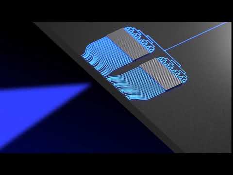
Blue optical phased array for augmented reality, trapped ion quantum computer and optogenetic neural stimulation.
New York, NY—March 19, 2020—While beam steering systems have been used for many years for applications such as imaging, display, and optical trapping, they require bulky mechanical mirrors and are overly sensitive to vibrations. Compact optical phased arrays (OPAs), which change the angle of an optical beam by changing the beam’s phase profile, are a promising new technology for many emerging applications. These include ultra-small solid-state LiDAR on autonomous vehicles, much smaller and lighter AR/VR displays, large-scale trapped-ion quantum computers to address ion qubits, and optogenetics, an emerging research field that uses light and genetic engineering to study the brain.
Long-range, high-performance OPAs require a large beam emission area densely packed with thousands of actively phase-controlled, power-hungry light-emitting elements. To date, such large-scale phased arrays for LiDAR have been impractical since the technologies in current use would have to operate at untenable electrical power levels.
Researchers led by Columbia Engineering Professor Michal Lipson have developed a low-power beam steering platform that is a non-mechanical, robust, and scalable approach to beam steering. The team is one of the first to demonstrate low-power large-scale optical phased array at near infrared and the first to demonstrate optical phased array technology on-chip at blue wavelength for autonomous navigation and augmented reality, respectively. In collaboration with Adam Kepecs' group at Washington University in St. Louis, the team has also developed an implantable photonic chip based on an optical switch array at blue wavelengths for precise optogenetic neural stimulation. The research has been recently published in three separate papers in Optica, Nature Biomedical Engineering, and Optics Letters.
“This new technology that enables our chip-based devices to point the beam anywhere we want opens the door wide for transforming a broad range of areas,” says Lipson, Eugene Higgins Professor of Electrical Engineering and Professor of Applied Physics. “These include, for instance, the ability to make LiDAR devices as small as a credit card for a self-driving car, or a neural probe that controls micron scale beams to stimulate neurons for optogenetics neuroscience research, or a light delivery method to each individual ion in a system for general quantum manipulations and readout.”
Lipson’s team has designed a multi-pass platform that reduces the power consumption of an optical phase shifter while maintaining both its operation speed and broadband low loss for enabling scalable optical systems. They let the light signal recycle through the same phase shifter multiple times so that the total power consumption is reduced by the same factor it recycles. They demonstrated a silicon photonic phased array containing 512 actively controlled phase shifters and optical antenna, consuming very low power while performing 2D beam steering over a wide field of view. Their results are a significant advance towards building scalable phased arrays containing thousands of active elements.
Phased array devices were initially developed at larger electromagnetic wavelengths. By applying different phases at each antenna, researchers can form a very directional beam by designing constructive interference in one direction and destructive in other directions. In order to steer or turn the beam’s direction, they can delay light in one emitter or shift a phase relative to another.
Current visible light applications for OPAs have been limited by bulky table-top devices that have a limited field of view due to their large pixel width. Previous OPA research done at the near-infrared wavelength, including work from the Lipson Nanophotonics Group, faced fabrication and material challenges in doing similar work at the visible wavelength.
“As the wavelength becomes smaller, the light becomes more sensitive to small changes such as fabrication errors,” says Min Chul Shin, a PhD student in the Lipson group and co-lead author of the Optics Letter paper. “It also scatters more, resulting in higher loss if fabrication is not perfect—and fabrication can never be perfect.”
It was only three years ago that Lipson’s team showed a low-loss material platform by optimizing fabrication recipes with silicon nitride. They leveraged this platform to realize their new beam steering system in the visible wavelength—the first chip-scale phased array operating at blue wavelengths using a silicon nitride platform.
A major challenge for the researchers was working in the blue range, which has the smallest wavelength in the visible spectrum and scatters more than other colors because it travels as shorter, smaller waves. Another challenge in demonstrating a phased array in blue was that to achieve a wide angle, the team had to overcome the challenge of placing emitters half a wavelength apart or at least smaller than a wavelength—40 nm spacing, 2,500 times smaller than human hair—which was very difficult to achieve. In addition, in order to make optical phased array useful for practical applications, they needed many emitters. Scaling this up to a large system would be extremely difficult.
“Not only is this fabrication really hard, but there would also be a lot of optical crosstalk with the waveguides that close,” says Shin. “We can’t have independent phase control plus we’d see all the light coupled to each other, not forming a directional beam.”
Solving these issues for blue meant that the team could easily do this for red and green, which have longer wavelengths. “This wavelength range enables us to address new applications such as optogenetic neural stimulation,” notes Aseema Mohanty, a postdoctoral research scientist and co-lead author of the Optics Letter and Nature Biomedical Engineering papers. “We used the same chip-scale technology to control an array of micron-scale beams to precisely probe neurons within the brain.”
The team is now collaborating with Applied Physics Professor Nanfang Yu’s group to optimize the electrical power consumption because low-power operation is crucial for lightweight head-mounted AR displays and optogenetics.
“We are very excited because we’ve basically designed a reconfigurable lens on a tiny chip on which we can steer the visible beam and change focus,” explains Lipson. “We have an aperture where we can synthesize any visible pattern we want every few tens of microseconds. This requires no moving parts and could be achieved at chip-scale. Our new approach means that we’ll be able to revolutionize augmented reality, optogenetics and many more technologies of the future.”
About the Studies
Journal: Optica
Title: Large-scale optical phased array using a low-power multi-pass silicon photonic platform
Authors: Steven A. Miller, You-Chia Chang, Christopher T. Phare, Min Chul Shin, Moshe Zadka, Samantha P. Roberts, Brian Stern, Xingchen Ji, Aseema Mohanty, Oscar A. Jimenez Gordillo, Utsav D. Dave, and Michal Lipson
This study was supported by Defense Advanced Research Projects Agency (HR0011-16-C-0107).
COI: S. A. M., C. T. P., M.L. holds individual ownership in a commercial entity; Y. C. C., S. P. R., B. S., M. L. are listed as inventors in a patent application related to this work, filed by Columbia University.
Journal: Nature Biomedical Engineering
Title: Reconfigurable nanophotonic silicon probes for sub-millisecond deep-brain optical stimulation
Authors: seema Mohanty, Qian Li, Mohammad Amin Tadayon, Samantha P. Roberts, Gaurang R. Bhatt, Euijae Shim, Xingchen Ji, Jaime Cardenas, Steven A. Miller, Adam Kepecs & Michal Lipson
This study was supported by National Science Foundation Brain EAGER (grant no. 1611090).
COI: .M., Q.L., M.A.T., X.J., A.K. and M.L. are listed as inventors in a patent application related to this work, filed by Columbia University. The remaining authors declare no competing interests.
Journal: Optics Letters
Title: Chip-scale Blue Light Phased Array
Authors: Min Chul Shin, Aseema Mohanty, Kyle Watson, Gaurang R. Bhatt, Christopher T. Phare, Steven A. Miller, Moshe Zadka, Brian S. Lee, Xingchen Ji, Ipshita Datta, and Michal Lipson
This study was supported by Defense Advanced Research Projects Agency (DARPA) (HR001110720034).
COI: MCS, AM, KW, ML are listed as inventors in a patent application related to this work, filed by Columbia University. The remaining authors declare no competing interests.
Columbia Engineering
Columbia Engineering, based in New York City, is one of the top engineering schools in the U.S. and one of the oldest in the nation. Also known as The Fu Foundation School of Engineering and Applied Science, the School expands knowledge and advances technology through the pioneering research of its more than 220 faculty, while educating undergraduate and graduate students in a collaborative environment to become leaders informed by a firm foundation in engineering. The School’s faculty are at the center of the University’s cross-disciplinary research, contributing to the Data Science Institute, Earth Institute, Zuckerman Mind Brain Behavior Institute, Precision Medicine Initiative, and the Columbia Nano Initiative. Guided by its strategic vision, “Columbia Engineering for Humanity,” the School aims to translate ideas into innovations that foster a sustainable, healthy, secure, connected, and creative humanity.
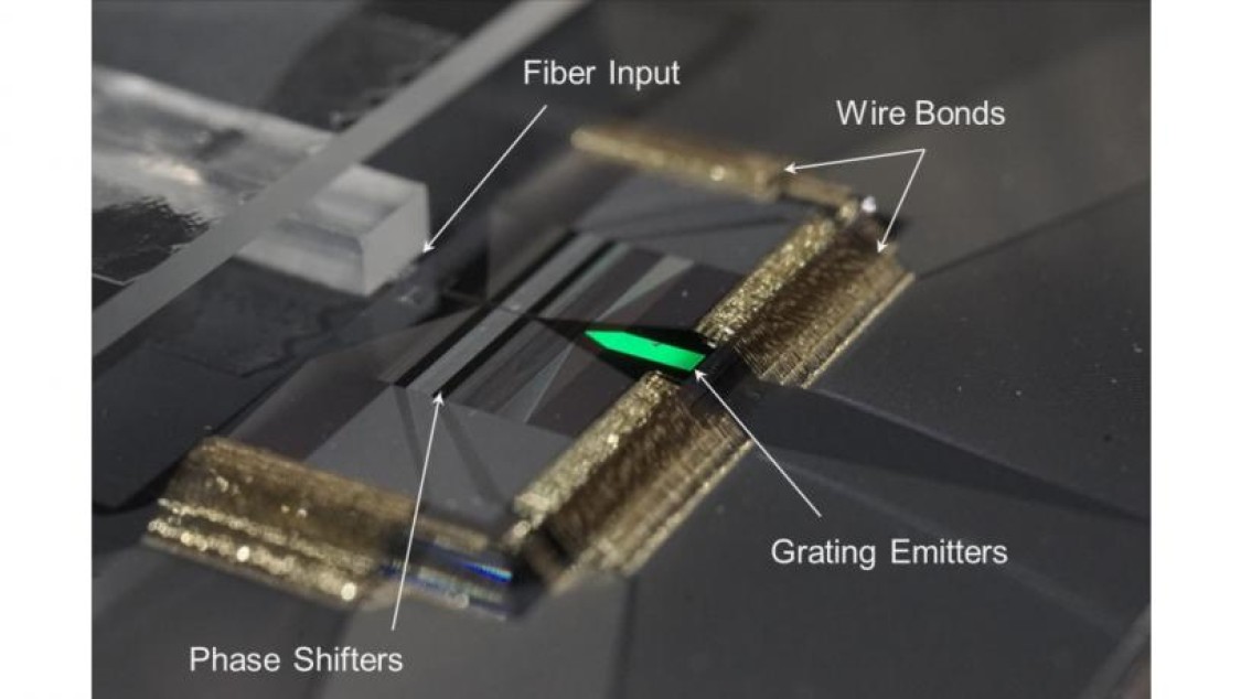
Header image: Implantable nanophotonic probe based on an optical switch array for optogenetic neural stimulation.
About the Study
Journal: Nature Human Behaviour
Title: “The direction of theta and alpha traveling waves modulates human memory processing”
Authors: Uma R. Mohan (1), Honghui Zhang (2), Bard Ermentrout (3), Joshua Jacobs (4,5)
- Surgical Neurology Branch, NINDS, National Institutes of Health
- Amazon Corporation, Seattle, Washington
- Department of Mathematics, University of Pittsburgh
- Department of Biomedical Engineering, Columbia University
- Department of Neurological Surgery, Columbia University
Funding: This work was supported by the DARPA Restoring Active Memory (RAM) program (Cooperative Agreement N66001-14-2-4032) and National Institutes of Health Grants R01-MH104606, U01-NS113198, RF1-MH114276, and the NationalScience Foundation (to Joshua Jacobs).
COI: The authors declare no competing interests.
Seeing More Deeply into Nanomaterials
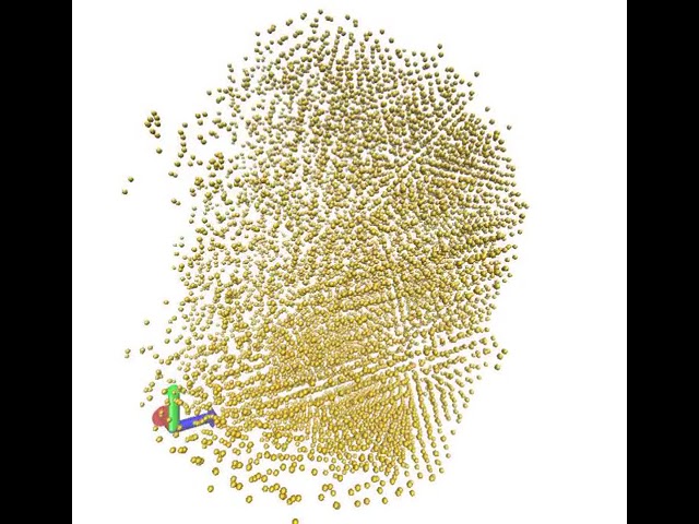
This video shows a 3D view of the reconstructed nanoparticles lattices with 360-degree rotation. Every golden dot represents one of the nanoparticles in the assembled structure. Credit: Oleg Gang/Columbia Engineering
Overcoming hurdles
To push through this challenge, the researchers discussed the various hurdles they needed to overcome. At the CFN and Columbia, the team had to figure out how they could build the structures with desired organization and how to convert them into an inorganic replica that can withstand powerful x-ray beams, while at NSLS-II the researchers had to tune the beamline by improving the resolution, data acquisition, and many other technical details.
“I think the best way to describe our progress is in terms of performance. When we first tried to take data at HXN, it took us three days and we got part of a data set. The second time we did this, it took us two days, and we got most of a whole data set, but our sample got destroyed in the process. By the third time it took a little over 24 hours, and we got a full data set. Each of these steps was about six months apart,” said Michelson.
Yan added: “Now we can finish it in a single day. The technique is mature enough that we also offer it to other users who would want to use our beamline to investigate their sample. Seeing into samples on this scale is interesting for fields such as microelectronics and battery research.”
The team leveraged the beamline’s abilities in two ways. They not only measured the phase contrast of the x-rays passing through the samples, but they also collected the x-ray fluorescence—the emitted light—from the sample. By measuring the phase contrast, the researchers could better distinguish the foreground from the background of their sample.
“Measuring the data was only half the battle; now we needed to translate the data into meaningful information about order and imperfection of self-assembled systems. We wanted to understand what type of defects can occur in these systems and what is their origin. Until this point, this information was only available through computation. Now we can really see this experimentally, which is super exciting and, literally, eye-opening for the future development of complex designed nanomaterials,” said Gang.
Seeing More Deeply into Nanomaterials
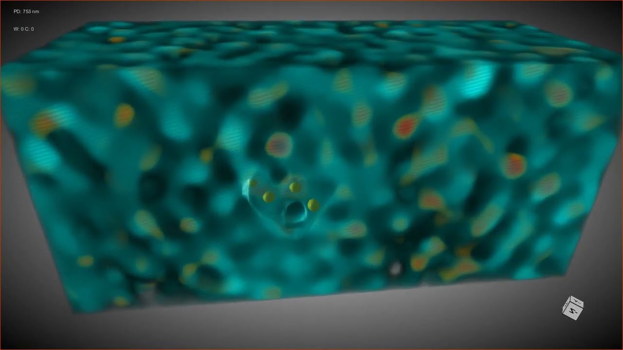
The multimaterial (iron/silica/platinum framework and gold nanoparticles lattice) reconstruction is viewed at a global level with some small region sectioned out and zoomed in for easier viewing of the structural motif of gold nanoparticles organized by tetrahedral frames in diamond lattice of nanoparticles and frames. Credit: Oleg Gang/Columbia Engineering
New software to better manage data
Together, the researchers developed new software tools to help untangle the large amount of data into chunks that could be processed and understood. One major challenge was being able to validate the resolution they achieved. The iterative process that finally led to the groundbreaking new resolution stretched over several months before the team had verified the resolution through both standard analysis and machine-learning approaches.
“It took my whole PhD to get here but I personally feel very gratified for being part of this collaboration. I was able to get involved in every step of the way from making the samples to running the beamline. All the new skills I have learned on this journey will be useful for everything that lies ahead,” said Michelson.
Pushing the boundaries
Even though the team has reached this impressive milestone, they are far from done. They already set their sights on the next steps to further push the boundaries of the possible.
“Now that we have gone through the data analysis process, we plan to make this part easier and faster for future projects, especially when further beamline improvements enable us to collect data even faster. The analysis is currently the bottleneck when doing high-resolution tomography work at HXN,” said Yan.
Gang added, “Aside from continuing to push the performance of the beamline, we also plan to use this new technique to dive deeper into the relationships between defects and properties of our materials. We plan to design more complex nanomaterials using DNA self-assembly that can be studied using HXN. In this way we can see how well the structure is built internally and connect this to the process of the assembly. We are developing a new bottom-up fabrication platform that we would not be able to image without this new capability.”
By understanding this connection between material’s properties and the assembly process, the researchers hope to unlock the path to fine-tuning these materials for future applications in designed nanomaterials for batteries and catalysis, for light manipulation, and for desired mechanical responses.
About the Study
Journal: Science
Title: Three-Dimensional Visualization of Nanoparticles Lattices and Multimaterial Frameworks
Authors: Aaron Michelson1 , Brian Minevich2 , Hamed Emamy2 , Xiaojing Huang3 , Yong S. Chu3 , Yan Hanfei3 , and Oleg Gang1,2,4
- Department of Applied Physics and Applied Mathematics, Columbia Engineering
- Department of Chemical Engineering, Columbia Engineering
- National Light Source II Brookhaven National Laboratory
- Center for Functional Nanomaterials, Brookhaven National Laboratory
The research to understand defects in DNA-assembled structures was supported by the US Department of Energy, Office of Basic Energy Sciences, Grant DE-SC0008772. Conversion of the DNA structures into inorganic replicas and structural analysis work was supported by the US Department of Defense, Army Research Office, W911NF-19-1-0395. Research to establish methods of tomography sample preparation, data collection, and data analysis was conducted at the Center for Functional Nanomaterials and the National Synchrotron Light Source II, which are U.S. Department of Energy Office of Science User Facilities at Brookhaven National Laboratory under Contract No. DE-SC0012704.
COI: The authors claim no competing interests.