At the Frontiers of Nanoengineering
Using Columbia’s nano facilities, over four hundred researchers have achieved nearly three hundred inventions and patents.
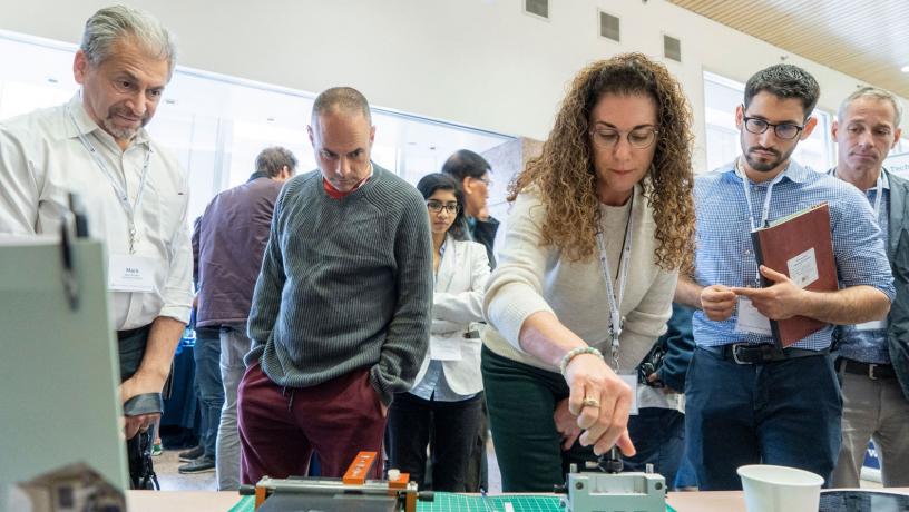
Attendees engaged with numerous presenters at the Columbia Nano Day poster session.
Through the interdisciplinary Columbia Nano Initiative (CNI), the university opens up its cutting-edge capabilities for engineering on the nanoscale to start-ups, industry and peers from academia. Over four hundred researchers, including members of 16 startups and dozens of other external groups, have utilized the recently-renovated 9000 square feet of shared lab space on campus, achieving nearly three hundred inventions and patents so far.
To celebrate that ongoing work, CNI hosted the first-ever Columbia Nano Day on October 29, convening a crowd of engineers, entrepreneurs, and scientists at Davis Auditorium to learn about the novel nanoscience and nanoengineering going on in Morningside Heights. Attendees heard presentations from faculty and staff, met members of companies working on campus to bring nanotech to market, and saw for themselves how facilities like the CNI Clean Room, the Electron Microscope Laboratory, and the Shared Materials Characterization Laboratory are enabling huge new possibilities in the tiniest of ways.
“It’s a highly collaborative effort,” noted Mary C. Boyce, Dean of Columbia Engineering. “You name the engineering field, and it’s being touched by nanoscience and requires nanotechnology to really push the frontiers. This deeply rich and innovative ecosystem has led to the creation of new, highly complex materials—materials that will form the foundation for transformative advances in electronics, medicine, energy, and entirely new applications not yet dreamed of.”
Several Columbia faculty spoke about how their research was supported by the facilities’ advanced technologies. Keren Bergman, Charles Batchelor Professor of Electrical Engineering, examined how progress in nanoscale photonics enables vastly more energy-efficient computing, while Michal Lipson, Eugene Higgins Professor of Electrical Engineering, talked about her work on next-generation silicon photonics providing high bandwidths at high speeds. Colin Nuckolls, Sheldon and Dorothea Buckler Professor of Chemistry, discussed interdisciplinary projects including creating single molecule electronics and developing programmable nanoscale objects to behave like atoms, and Ken Shepard, Lau Family Professor of Electrical Engineering, explained how he fashions direct interfaces between integrated circuit chips and biological systems like the brain.
Then, Pravina Raghavan, EVP for Small Business Services and Community Economic Development at New York Empire State Development, moderated a panel featuring four scientist-entrepreneurs who use CNI facilities to bring their products to market.
“Being able to put off investing in certain equipment because we could use it here was a big help,” said Patrick Truitt, principal scientist at SeeQC, which is developing superconducting quantum technologies for information processing.
“CNI didn’t just make things easier for us, it made things possible for us,” said Nicholas Manousos, co-founder of Firehouse Horology, which makes parts for mechanical wristwatches using nanofabrication techniques. “We could not do what we do if it wasn’t for the fabulous resources we have here.”
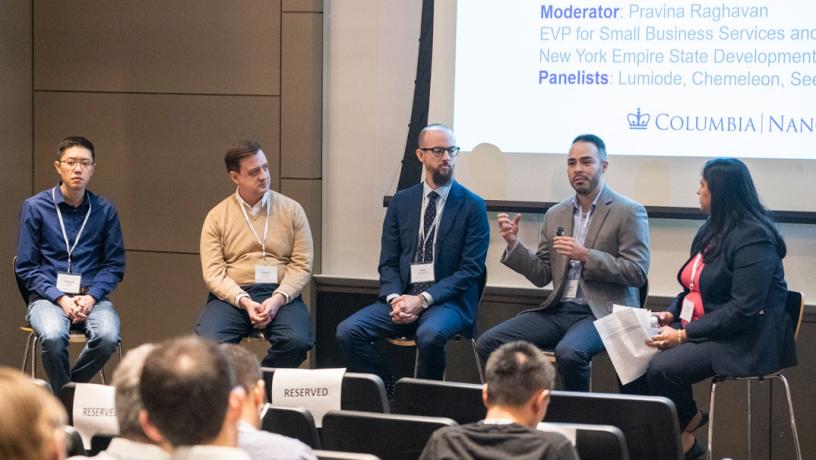
NY state official Pravina Raghavan moderated a panel with scientist-entrepreneurs who use CNI facilities to bring their products to market.
CNI didn’t just make things easier for us, it made things possible for us.
Before leading lab tours, the scientists who oversee them enumerated the facilities’ formidable array of equipment and expertise. Nava Ariel-Sternberg, director of CNI Shared Labs, explained that the lab space is just the beginning, and the initiative also offers dedicated meetings, seminars, and assistance from a professional staff dedicated to CNI projects. Amir Zangiabadi and Daniel Paley, directors of Electron Microscopy Labs and the Shared Materials Characterization Lab, respectively, described some of the new analysis techniques in their labs, featuring examples from research projects and their specific data analyses approaches.
The day also included a poster session showcasing student research and plenty of time for questions and answers.
“With this promise to deliver revolutionary technologies that can transform computation, communications, and sensing, nanotechnology and quantum materials research are really a top priority for the university,” said Peter de Menocal, Dean of Science in the Faculty of Arts and Sciences. “Columbia’s commitment to cutting-edge research and instrumentation has never been stronger, we’re really trying to put every bit of horsepower we can into this initiative. This is where the world is headed.”