
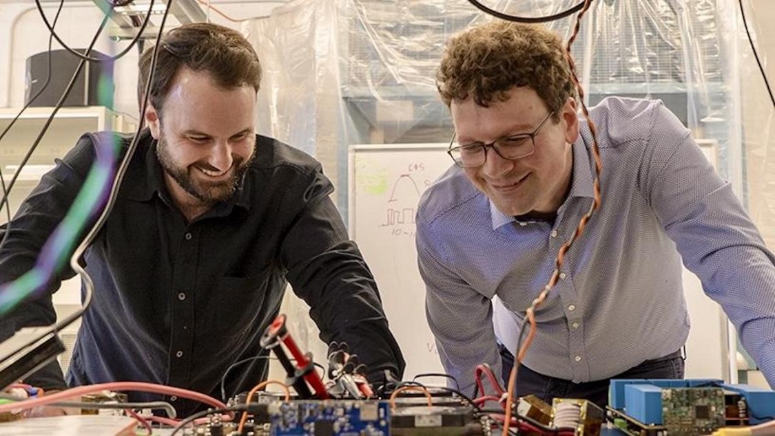
Columbia and Tau have been longtime partners. The two have collaborated through Preindl, a leader in designing next-generation power converters, and his Motor Drives and Power Electronics Laboratory (MPlab) to design modern power electronic converters and motor drive solutions that are not only high-performance, but also scalable.
Their groundbreaking collaborative work has been recognized across academia and industry for pioneering the field of software-defined power conversion, dating back in part to Preindl’s NSF CAREER Award. The collaboration has been celebrated through a number of awards including Autotech Breakthrough’s V2X and V2I Innovation of the Year Awards, Fast Company World Changing Ideas recognition, and Fast Company’s Best Workplace for Innovators (2023, 2024). The Center provides a platform to further advance their work together at a new scale.
“Our vision is to ‘electrify humanity,’” Preindl said. “Our Center will build advanced energy conversion technologies that enable electrification of energy systems and scale electrification at unprecedented levels.”
Focus of the Center
The Center will focus on research in electric energy conversion and leverage advanced power electronics, novel topologies for power converters, modern and distributed control, and machine learning/artificial intelligence to enable reliable and resilient solutions that facilitate a circular economy. In doing so, researchers are also actively working to limit the use of materials adversely affecting the environment, such as rare earth elements or critical minerals.
The Center will engineer solutions for sustainable electric transportation and energy systems. Target applications include electric drivetrains, propulsion systems, and electric supply infrastructure; distributed energy resources such as renewable energy and battery storage for the electric grid; and emerging electric loads including data centers and heating electrification.
The Center also intends to support the translation of outcomes to industrial applications to maximize the impact through strategic technology development and transfer.
Finally, the Center plans to support the training of highly qualified engineers and scientists in the field and provide mentorship and career development for students and researchers engaging with the Center.
“We are excited to deepen our partnership with both Columbia and Dr. Preindl through the founding of the Center alongside Tau,” said Wesley Pennington, Tau’s founder and CEO. “We have an established and celebrated history of leading research and innovation together with the university and look forward to deepening our collaboration to further accelerate the electrification of the world. The Center of Advanced Electrification in collaboration with Tau Motors will provide a larger platform to continue to invent, develop, translate, and deploy technologies that accelerate the energy transition, as well as train and build future leaders to extend our mission as we solve some of the world’s most pressing challenges.”
Future Center activities
The Center team is already planning a broad range of activities rooted in scientific innovation and technical advancement of the field. In addition to research and innovation activities, the Center is developing programs including the organization of an annual symposium to foster technical discussions and interactions between faculty and industry. They are also developing a seminar series with invited external speakers, as well as student activities, such as recruiting events.
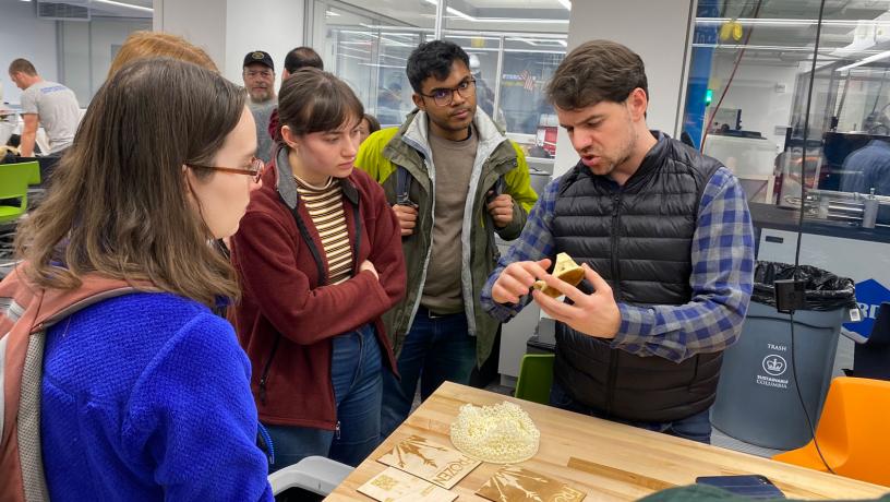
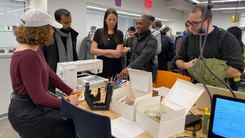
Columbia University's Makerspace
Explore the innovative hub for creativity and learning at Columbia University's Makerspace.
New York, NY—May 17, 2019—Semiconductors, which are the basic building blocks of transistors, microprocessors, lasers, and LEDs, have driven advances in computing, memory, communications, and lighting technologies since the mid-20th century. Recently discovered two-dimensional (2D) materials, which feature many superlative properties, have the potential to advance these technologies, but creating 2D devices with both good electrical contacts and stable performance has proved challenging.
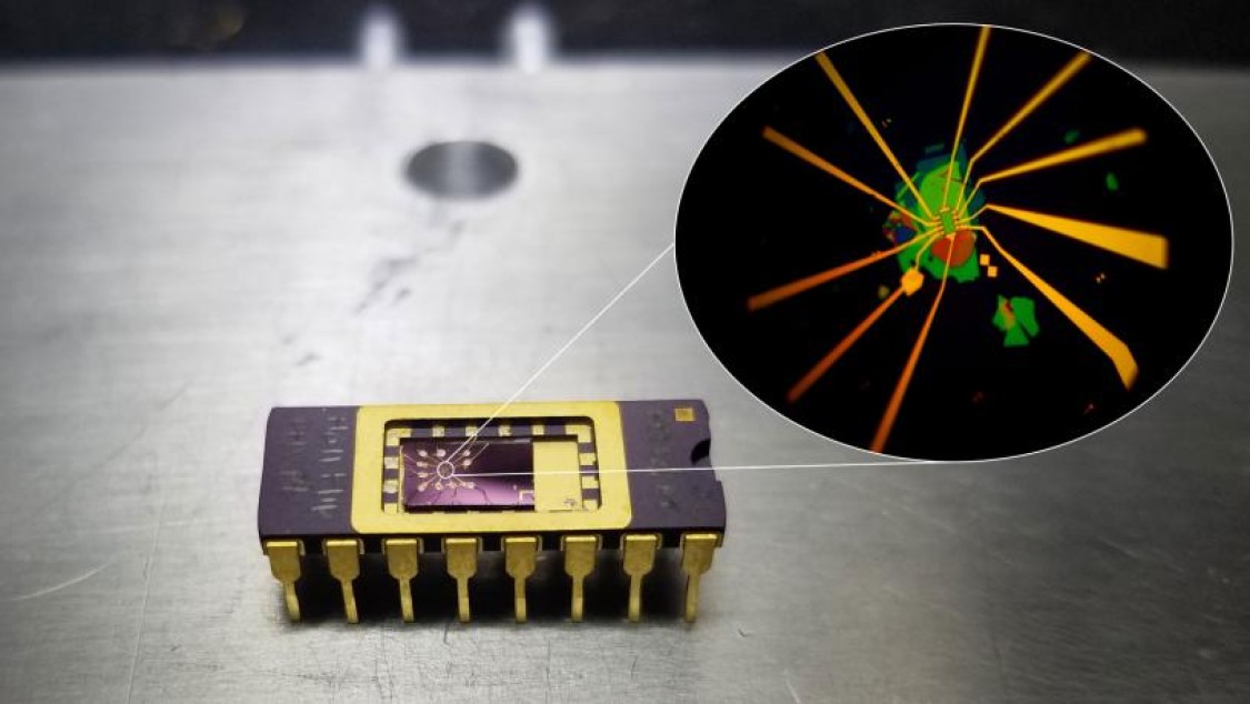
Researchers at Columbia Engineering report that they have demonstrated a nearly ideal transistor made from a two-dimensional material stack—with only a two-atom-thick semiconducting layer—by developing a completely clean and damage-free fabrication process. Their method shows vastly improved performance compared to 2D semiconductors fabricated with a conventional process, and could provide a scalable platform for creating ultra-clean devices in the future. The study was published today in Nature Electronics.
“Making devices out of 2D materials is a messy business,” says James Teherani, assistant professor of electrical engineering. “Devices vary wildly from run to run and often degrade so fast that you see performance diminish while you’re still measuring them.”
Having grown tired of the inconsistent results, Teherani’s team set out to develop a better way to make stable devices. “So,” he explains, “we decided to separate the pristine device from the dirty fabrication processes that lead to variability.”
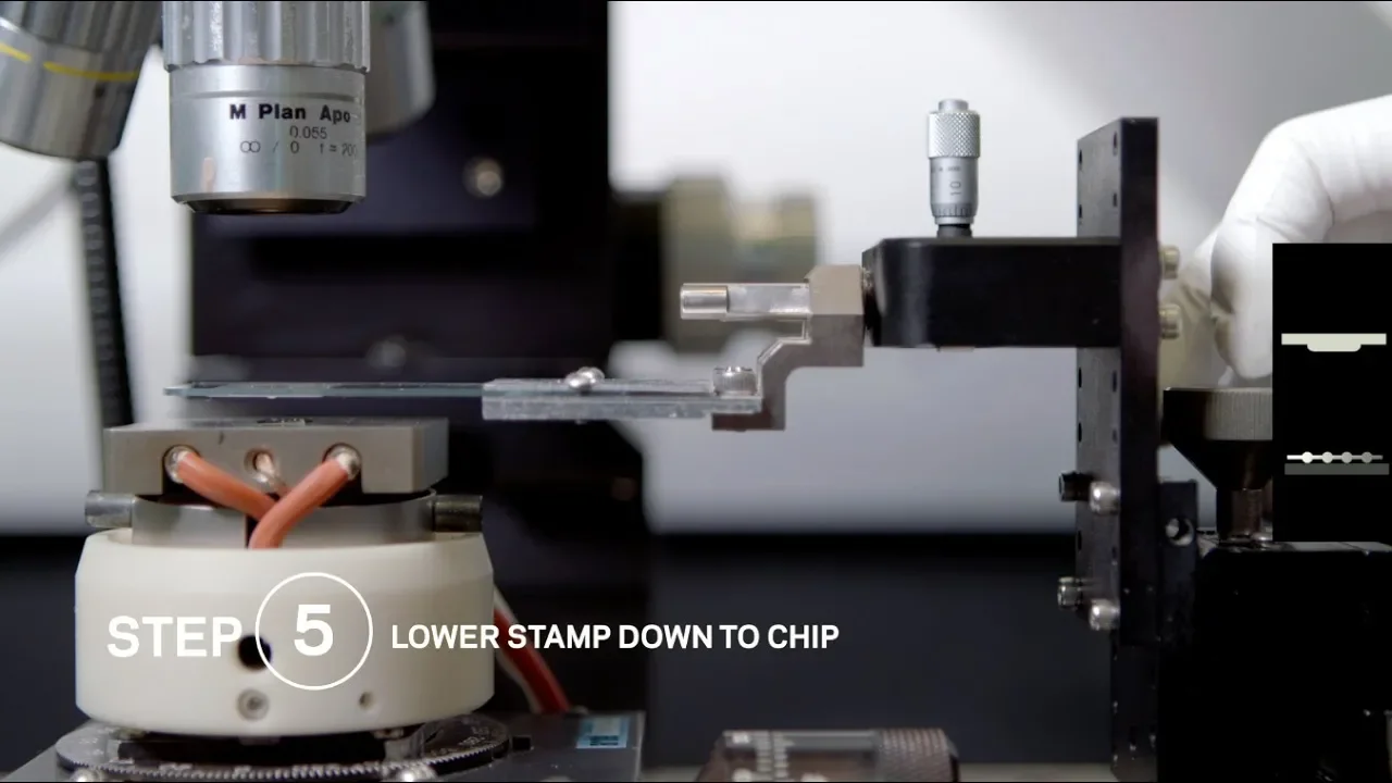
As shown in this new study, Teherani and his colleagues developed a two-step, ultra-clean nanofabrication process that separates the “messy” steps of fabrication—those that involve “dirty” metallization, chemicals, and polymers used to form electrical connections to the device—from the active semiconductor layer. Once they complete the messy fabrication, they could pick up the contacts and transfer them onto the clean active device layer, preserving the integrity of both layers.
“The thinness of these semiconductors is a blessing and a curse,” says Teherani. “While the thinness allows them to be transparent and to be picked up and placed wherever you want them, the thinness also means there's nearly zero volume—the device is almost entirely surface. Because of this, any surface dirt or contamination will really degrade a device.”
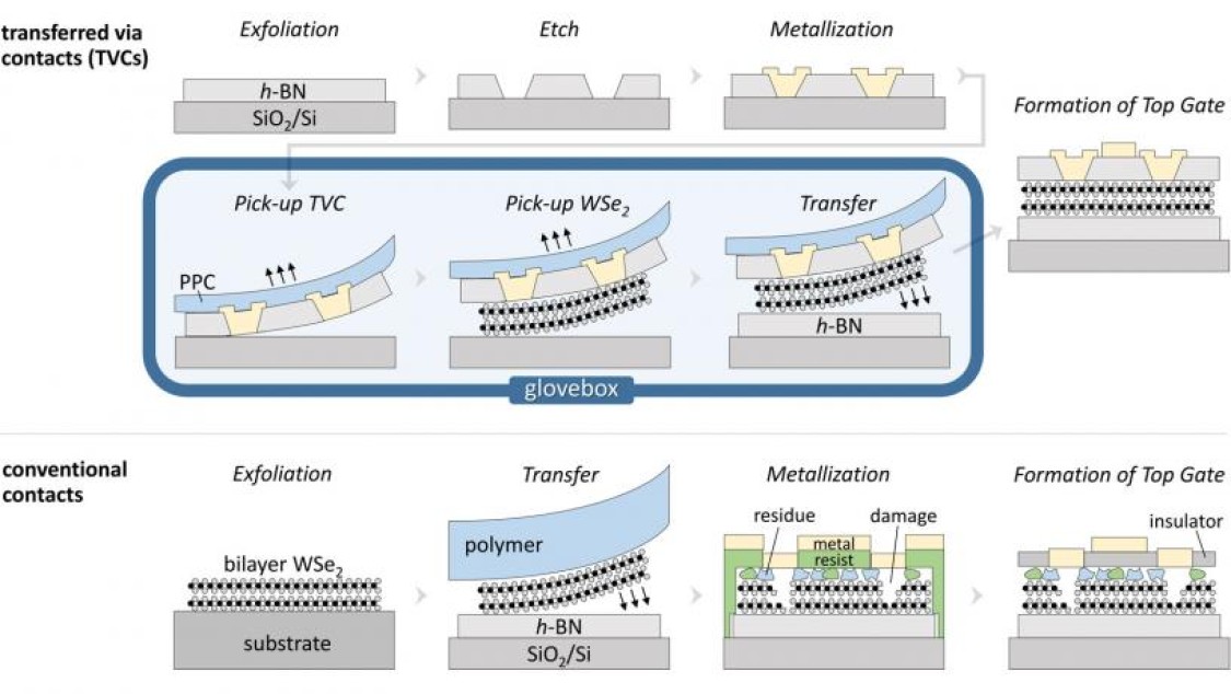
Currently, most devices are not encapsulated with a layer that protects the surface and contacts from contamination during fabrication. Teherani’s team showed that their method can now not only protect the semiconductor layer so that they don't see performance degradation over time, but it can also yield high performance devices.
Teherani collaborated with Jim Hone, Wang Fong-Jen Professor of Mechanical Engineering, making use of the fabrication and analysis facilities of the Columbia Nano Initiative and the National Science Foundation-funded Materials Research Science and Engineering Center at Columbia. The team made the transferred contacts from metal embedded in insulating hexagonal boron nitride (h-BN) outside a glovebox and then dry-transferred the contact layer onto the 2D semiconductor, which was kept pristine inside a nitrogen glovebox. This process prevents direct-metallization-induced damage while simultaneously providing encapsulation to protect the device.
Video on the differences between 2D and 3D material

Video on the step-by-step nanofabrication of 2D material stacks
Now that the researchers have developed a stable, repeatable process, they are using the platform to make devices that can move out of the lab into real-world engineering problems.
“The development of high performance 2D devices requires advances in the semiconductor materials from which they are made,” Teherani adds. “More precise tools like ours will enable us to build more complex structures with potentially greater functionality and better performance.”
Columbia Engineering
Columbia Engineering, based in New York City, is one of the top engineering schools in the U.S. and one of the oldest in the nation. Also known as The Fu Foundation School of Engineering and Applied Science, the School expands knowledge and advances technology through the pioneering research of its more than 220 faculty, while educating undergraduate and graduate students in a collaborative environment to become leaders informed by a firm foundation in engineering. The School’s faculty are at the center of the University’s cross-disciplinary research, contributing to the Data Science Institute, Earth Institute, Zuckerman Mind Brain Behavior Institute, Precision Medicine Initiative, and the Columbia Nano Initiative. Guided by its strategic vision, “Columbia Engineering for Humanity,” the School aims to translate ideas into innovations that foster a sustainable, healthy, secure, connected, and creative humanity.