Nano-objects of Desire: Assembling Ordered Nanostructures in 3-D

Research from the Gang lab

Sakul Ratanalert


Seeing More Deeply into Nanomaterials
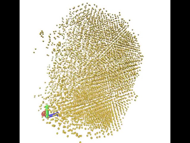
This video shows a 3D view of the reconstructed nanoparticles lattices with 360-degree rotation. Every golden dot represents one of the nanoparticles in the assembled structure. Credit: Oleg Gang/Columbia Engineering
Overcoming hurdles
To push through this challenge, the researchers discussed the various hurdles they needed to overcome. At the CFN and Columbia, the team had to figure out how they could build the structures with desired organization and how to convert them into an inorganic replica that can withstand powerful x-ray beams, while at NSLS-II the researchers had to tune the beamline by improving the resolution, data acquisition, and many other technical details.
“I think the best way to describe our progress is in terms of performance. When we first tried to take data at HXN, it took us three days and we got part of a data set. The second time we did this, it took us two days, and we got most of a whole data set, but our sample got destroyed in the process. By the third time it took a little over 24 hours, and we got a full data set. Each of these steps was about six months apart,” said Michelson.
Yan added: “Now we can finish it in a single day. The technique is mature enough that we also offer it to other users who would want to use our beamline to investigate their sample. Seeing into samples on this scale is interesting for fields such as microelectronics and battery research.”
The team leveraged the beamline’s abilities in two ways. They not only measured the phase contrast of the x-rays passing through the samples, but they also collected the x-ray fluorescence—the emitted light—from the sample. By measuring the phase contrast, the researchers could better distinguish the foreground from the background of their sample.
“Measuring the data was only half the battle; now we needed to translate the data into meaningful information about order and imperfection of self-assembled systems. We wanted to understand what type of defects can occur in these systems and what is their origin. Until this point, this information was only available through computation. Now we can really see this experimentally, which is super exciting and, literally, eye-opening for the future development of complex designed nanomaterials,” said Gang.
Seeing More Deeply into Nanomaterials
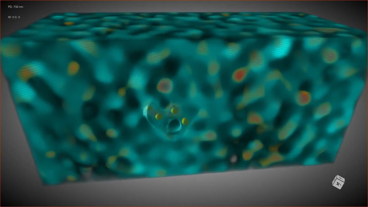
The multimaterial (iron/silica/platinum framework and gold nanoparticles lattice) reconstruction is viewed at a global level with some small region sectioned out and zoomed in for easier viewing of the structural motif of gold nanoparticles organized by tetrahedral frames in diamond lattice of nanoparticles and frames. Credit: Oleg Gang/Columbia Engineering
New software to better manage data
Together, the researchers developed new software tools to help untangle the large amount of data into chunks that could be processed and understood. One major challenge was being able to validate the resolution they achieved. The iterative process that finally led to the groundbreaking new resolution stretched over several months before the team had verified the resolution through both standard analysis and machine-learning approaches.
“It took my whole PhD to get here but I personally feel very gratified for being part of this collaboration. I was able to get involved in every step of the way from making the samples to running the beamline. All the new skills I have learned on this journey will be useful for everything that lies ahead,” said Michelson.
Pushing the boundaries
Even though the team has reached this impressive milestone, they are far from done. They already set their sights on the next steps to further push the boundaries of the possible.
“Now that we have gone through the data analysis process, we plan to make this part easier and faster for future projects, especially when further beamline improvements enable us to collect data even faster. The analysis is currently the bottleneck when doing high-resolution tomography work at HXN,” said Yan.
Gang added, “Aside from continuing to push the performance of the beamline, we also plan to use this new technique to dive deeper into the relationships between defects and properties of our materials. We plan to design more complex nanomaterials using DNA self-assembly that can be studied using HXN. In this way we can see how well the structure is built internally and connect this to the process of the assembly. We are developing a new bottom-up fabrication platform that we would not be able to image without this new capability.”
By understanding this connection between material’s properties and the assembly process, the researchers hope to unlock the path to fine-tuning these materials for future applications in designed nanomaterials for batteries and catalysis, for light manipulation, and for desired mechanical responses.
About the Study
Journal: Science
Title: Three-Dimensional Visualization of Nanoparticles Lattices and Multimaterial Frameworks
Authors: Aaron Michelson1 , Brian Minevich2 , Hamed Emamy2 , Xiaojing Huang3 , Yong S. Chu3 , Yan Hanfei3 , and Oleg Gang1,2,4
- Department of Applied Physics and Applied Mathematics, Columbia Engineering
- Department of Chemical Engineering, Columbia Engineering
- National Light Source II Brookhaven National Laboratory
- Center for Functional Nanomaterials, Brookhaven National Laboratory
The research to understand defects in DNA-assembled structures was supported by the US Department of Energy, Office of Basic Energy Sciences, Grant DE-SC0008772. Conversion of the DNA structures into inorganic replicas and structural analysis work was supported by the US Department of Defense, Army Research Office, W911NF-19-1-0395. Research to establish methods of tomography sample preparation, data collection, and data analysis was conducted at the Center for Functional Nanomaterials and the National Synchrotron Light Source II, which are U.S. Department of Energy Office of Science User Facilities at Brookhaven National Laboratory under Contract No. DE-SC0012704.
COI: The authors claim no competing interests.