Video describing the development of e-IGTs, biocompatible ion-driven soft transistors that can perform real-time neurologically relevant computation.

Conventional transistors are made out of silicon, so they cannot function in the presence of ions and water, and in fact break down because of ion diffusion into the device. Therefore, the devices need to be fully encapsulated in the body, usually in metal or plastic. Moreover, although they work well with electrons, they are not very effective at interacting with ionic signals, which is how the body’s cells communicate. As a result, these properties restrict the abiotic/biotic coupling to capacitive interactions only on the surface of material, resulting in lower performance. Organic materials have been used to overcome these limitations as they are inherently flexible, but the electrical performance of these devices was not sufficient to perform real-time brain signal recording and processing.
Khodagholy’s team took advantage of both the electronic and the ionic conduction of organic materials to create ion driven transistors they call e-IGTs, or enhancement-mode, internal ion-gated organic electrochemical transistors, that have embedded mobile ions inside their channels. Because the ions do not need to travel long distances to participate in the channel switching process, they can be switched on and off quickly and efficiently. The transient responses depend on electron hole rather than ion mobility, and combine with high transconductance to result in a gain-bandwidth that is several orders of magnitude above that of other ion-based transistors.
The researchers used their e-IGTs to acquire a wide range of electrophysiological signals, such as in vivo recording of neural action impulses, and to create soft, biocompatible, long-term implantable neural processing units for the real-time detection of epileptic discharges.
“We’re excited about these findings,” says Gelinas. “We’ve shown that E-IGTs offer a safe, reliable, and high-performance building block for chronically implanted bioelectronics, and I am optimistic that these devices will enable us to safely expand how we use bioelectronic devices to address neurologic disease.”
Another major advance is demonstrated by the researchers in their Science Advances paper: enabling bioelectronic devices, specifically those implanted in the body for diagnostics or therapy, to interface effectively and safely with human tissue, while also making them capable of performing complex processing. Inspired by electrically active cells, similar to those in the brain that communicate with electrical pulses, the team created a single material capable of performing multiple, non-linear, dynamic electronic functions just by varying the size and density of its composite mixed-conducting particles.
Video describing the development of MCPs, mixed-conducting particulate composites that allow creation of electronic components out of a single material.

“This innovation opens the door to a fundamentally different approach to electronic device design, mimicking biological networks and creating multifunctional circuits from purely biodegradable and biocompatible components,” says Khodagholy.
The researchers designed and created mixed conducting particulate (MCP)-based high performance anisotropic films, independently addressable transistors, resistors, and diodes that are pattern-free, scalable, and biocompatible. These devices carried out a variety of functions, including recording neurophysiologic activity from individual neurons, performing circuit operations, and bonding high-resolution soft and rigid electronics.
“MCP substantially reduces the footprint of neural interface devices, permitting recording of high-quality neurophysiological data even when the amount of tissue exposed is very small, and thus decreases the risk of surgical complications,” says Gelinas. “And because MCP is composed of only biocompatible and commercially available materials, it will be much easier to translate into biomedical devices and medicine.”
Both the E-IGTs and MCP hold great promise as critical components of bioelectronics, from wearable miniaturized sensors to responsive neurostimulators. The E-IGTs can be manufactured in large quantities and are accessible to a broad range of fabrication processes. Similarly, MCP components are inexpensive and easily accessible to materials scientists and engineers. In combination, they form the foundation for fully implantable biocompatible devices that can be harnessed both to benefit health and to treat disease.
Khodagholy and Gelinas are now working on translating these components into functional long-term implantable devices that can record and modulate brain activity to help patients with neurological diseases such as epilepsy.
“Our ultimate goal is to create accessible bioelectronic devices that can improve peoples’ quality of life,” says Khodagholy, “and with these new materials and components, it feels like we have stepped closer to that.”
Columbia Engineering
Columbia Engineering, based in New York City, is one of the top engineering schools in the U.S. and one of the oldest in the nation. Also known as The Fu Foundation School of Engineering and Applied Science, the School expands knowledge and advances technology through the pioneering research of its more than 220 faculty, while educating undergraduate and graduate students in a collaborative environment to become leaders informed by a firm foundation in engineering. The School’s faculty are at the center of the University’s cross-disciplinary research, contributing to the Data Science Institute, Earth Institute, Zuckerman Mind Brain Behavior Institute, Precision Medicine Initiative, and the Columbia Nano Initiative. Guided by its strategic vision, “Columbia Engineering for Humanity,” the School aims to translate ideas into innovations that foster a sustainable, healthy, secure, connected, and creative humanity.
A Tactile Finger based on Optical Signals
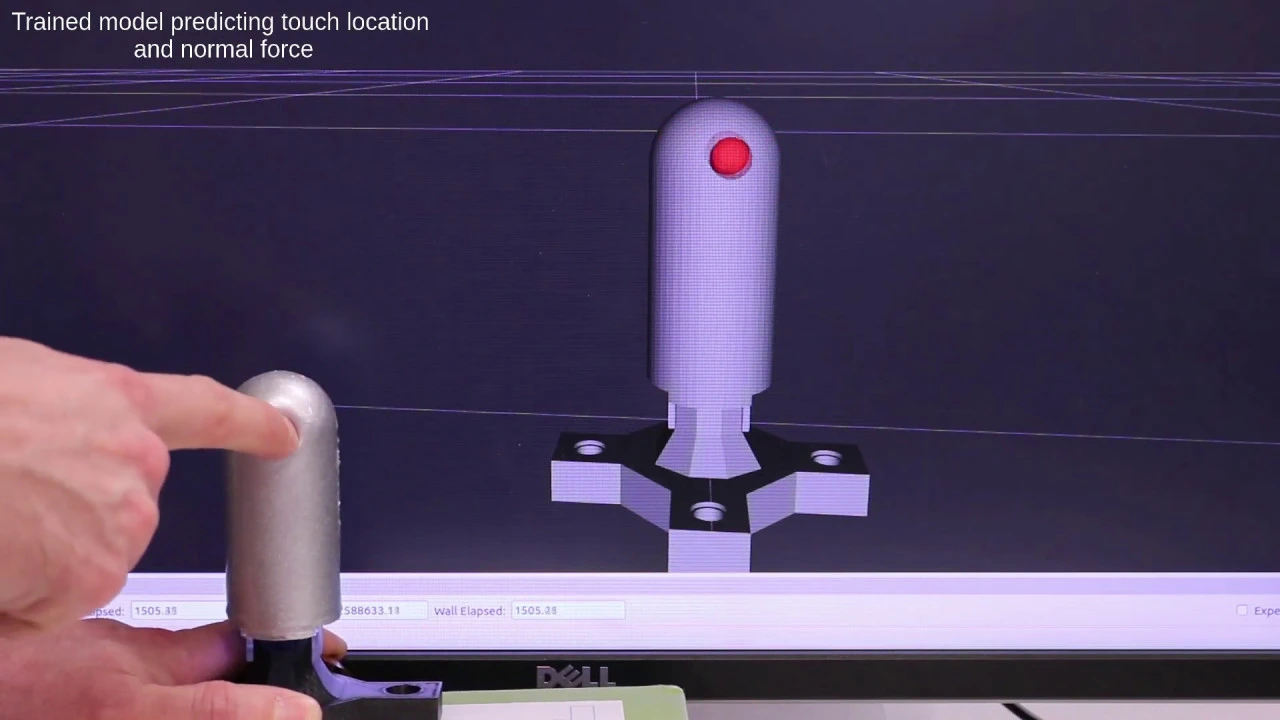
The study, led by students Pedro Piacenza and Keith Behrman, was published online in IEEE/ASME Transactions on Mechatronics. It demonstrates the two aspects of the underlying technology that combine to enable the new results. Firstly, in this project, the researchers use light to sense touch. Under the “skin,” their finger has a layer made of transparent silicone, into which they shined light from more than 30 LEDs. The finger also has more than 30 photodiodes that measure how the light bounces around. Whenever the finger touches something, its skin deforms, so light shifts around in the transparent layer underneath. Measuring how much light goes from every LED to every diode, the researchers end up with close to 1,000 signals that each contain some information about the contact that was made. Since light can also bounce around in a curved space, these signals can cover a complex 3D shape such as a fingertip.
“The human finger provides incredibly rich contact information--more than 400 tiny touch sensors in every square centimeter of skin!” says Ciocarlie. “That was the model that pushed us to try and get as much data as possible from our finger. It was critical to be sure all contacts on all sides of the finger were covered--we essentially built a tactile robot finger with no blind spots.”
Secondly, the team designed this data to be processed by machine learning algorithms. Because there are so many signals, all of them partially overlapping with each other, the data is too complex to be interpreted by humans. Fortunately, current machine learning techniques can learn to extract the information that researchers care about: where the finger is being touched, what it is touching the finger, how much force is being applied, etc.
“Our results show that a deep neural network can extract this information with very high accuracy,” says Kymissis, who is also a member of the Data Science Institute. “Our device is truly a tactile finger designed from the very beginning to be used in conjunction with AI algorithms.”
In addition, the team built the finger so it, and others, can be put onto robotic hands. Integrating the system onto a hand is easy: thanks to this new technology, the finger collects almost 1,000 signals, but only needs a 14-wire cable connecting it to the hand, and it needs no complex off-board electronics. The researchers already have two dexterous hands (capable of grasping and manipulating objects) in their lab being outfitted with these fingers--one hand has three fingers, and the other one four. In the next months, the team will be using these hands to try and demonstrate dexterous manipulation abilities, based on tactile and proprioceptive data.
“Dexterous robotic manipulation is needed now in fields such as manufacturing and logistics, and is one of the technologies that, in the longer term, are needed to enable personal robotic assistance in other areas, such as healthcare or service domains,” Ciocarlie adds.
Columbia Engineering
Columbia Engineering, based in New York City, is one of the top engineering schools in the U.S. and one of the oldest in the nation. Also known as The Fu Foundation School of Engineering and Applied Science, the School expands knowledge and advances technology through the pioneering research of its more than 220 faculty, while educating undergraduate and graduate students in a collaborative environment to become leaders informed by a firm foundation in engineering. The School’s faculty are at the center of the University’s cross-disciplinary research, contributing to the Data Science Institute, Earth Institute, Zuckerman Mind Brain Behavior Institute, Precision Medicine Initiative, and the Columbia Nano Initiative. Guided by its strategic vision, “Columbia Engineering for Humanity,” the School aims to translate ideas into innovations that foster a sustainable, healthy, secure, connected, and creative humanity.
About the Study
The study is titled “A Sensorized Multicurved Robot Finger with Datadriven Touch Sensing via Overlapping Light Signals.”
Authors are: Pedro Piacenza and Matei Ciocarlie, Mechanical Engineering; Keith Behrman and Ioannis Kymissis, Electrical Engineering; and Benedikt Schifferer, Computer Science.
The work was sponsored in part by the National Science Foundation, under its CAREER program (grant IIS-1551631) and a National Robotics Initiative (grant CMMI-1734557).
The authors declare no financial or other conflicts of interest.
Clinical demonstration of 3D arrhythmia mapping using Electromechanical Wave Imaging
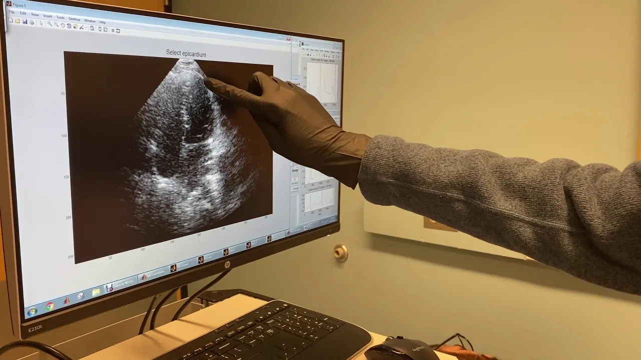
The researchers ran a double-blinded clinical study to evaluate the diagnostic accuracy of EWI for localizing and identifying the sites of atrial and ventricular arrhythmias. Fifty-five patients, who had pre-existing cardiac disease including previous catheter ablations and/or other cardiovascular co-morbidities, underwent EWI scans prior to their catheter ablation procedures to generate activation maps of their hearts. The team retrospectively compared EWI maps and 12-lead ECG assessments made by six expert electrophysiologists in a team led by Wan to the site of successful ablation found on the intracardiac electroanatomical maps obtained during invasive catheter mapping.
“The accuracy of EWI was higher than that of clinical diagnosis by electrophysiologists reading standard 12-lead ECGs,” says the study’s co-first author Lea Melki, a PhD student in the department of biomedical engineering working in Konofagou’s team who teamed up with electrophysiology fellow and co-first author, Chris Grubb, to accomplish that task. “While the inter-observer variability of our expert electrophysiologists may have played a role, we also know that 12-lead ECGs are limited in diagnosing arrhythmias from the posterior side of the heart, while EWI allows for easier anatomical location in 3D. In fact, a big advantage of EWI is the ease with which activation maps can clearly demarcate the earliest sites of interest along with direct anatomic visualization using standard echocardiography scans that clinicians are already trained on.”
The researchers are now planning a long-term clinical study, set to start later this year that will use EWI prediction to improve ablation outcomes by increasing the accuracy of the ablation site and spare normal tissue from ablation.
“It’s really clear now that, when used in conjunction with standard 12-lead ECG, EWI can be a valuable tool for diagnosis, clinical decision making, and treatment planning of patients with arrhythmias,” says Melki. “We believe our EWI technique, with minimal training, will result in higher accuracy in the site of ablation, a faster procedure, and fewer complications and repeat visits after the procedure. This is a win-win for everyone, both patients and clinicians.”
Columbia Engineering
Columbia Engineering, based in New York City, is one of the top engineering schools in the U.S. and one of the oldest in the nation. Also known as The Fu Foundation School of Engineering and Applied Science, the School expands knowledge and advances technology through the pioneering research of its more than 220 faculty, while educating undergraduate and graduate students in a collaborative environment to become leaders informed by a firm foundation in engineering. The School’s faculty are at the center of the University’s cross-disciplinary research, contributing to the Data Science Institute, Earth Institute, Zuckerman Mind Brain Behavior Institute, Precision Medicine Initiative, and the Columbia Nano Initiative. Guided by its strategic vision, “Columbia Engineering for Humanity,” the School aims to translate ideas into innovations that foster a sustainable, healthy, secure, connected, and creative humanity.
Lead Image Caption: Electromechanical wave imaging (EWI) activation maps are capable of localizing the arrhythmic origin and differentiating irregular beats (figure 2) from consecutive normal sinus rhythm beats (figure 1) on the same patient before ablation. Red illustrates early and blue represents late activation (in milliseconds). The red arrow indicates the earliest activated region displayed by EWI, which successfully corresponds to the source of the arrhythmia in agreement with the site that was ablated with the intracardiac ablation site. LV = left ventricle, RV = left ventricle, ANT = anterior, POST = posterior.
Journal
Science Translational Medicine
About the Study
The study is titled “Noninvasive localization of cardiac arrhythmias using electromechanical wave imaging.”
Authors are: Christopher S. Grubb 1, Lea Melki 2, Daniel Y. Wang 1, James Peacock 1, Jose Dizon 1, Vivek Iyer 1, Carmine Sorbera 1, Angelo Biviano 1, David A. Rubin 1, John P. Morrow 1, Deepak Saluja 1, Andrew Tieu2 , Pierre Nauleau 2, Rachel Weber 2, Salma Chaudhary 1, Irfan Khurram 1, Marc Waase 1, Hasan Garan 1, Elisa E Konofagou 2,3, and Elaine Y. Wan 1.
1 Division of Cardiology, Department of Medicine, Vagelos College of Physicians and Surgeons, Columbia University, New York, NY 10032
2 Ultrasound Elasticity Imaging Laboratory, Department of Biomedical Engineering, Columbia University, New York, NY 10032
3 Department of Radiology, Columbia University Medical Center, New York, NY 10032
The study was supported by the National Institutes of Health (NIH R01 HL140646-01, R01 HL114358, and R01 EB006042).
The authors declare no financial or other conflicts of interest.